- Home
-
Products
- Functional Crystals
- Crystal Substrates
- Sputtering Targets
- Powder, Sputtering Sources
- Metal Crystals
- Coated Wafers
- Glass/Ceramic Substrates
- Mat. Processing, Equipment Service
- Services
-
Application
- Partner
- Media
- Contact Us
- About Us
- Home
- Products
- Coated Wafers
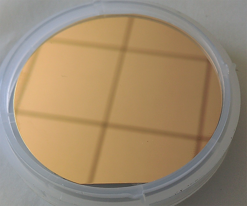
- Au/Cr/Si
- Functional Crystals
- Crystal Substrates
- Sputtering Targets
- Powder, Sputtering Sources
- Metal Crystals
- Coated Wafers
- Glass/Ceramic Substrates
- Mat. Processing, Equipment Service
Au/Cr/Si
Epitaxial wafer (EPI) refers to the semiconductor thin film grown on the substrate. The thin film is mainly composed of p-type, quantum well and n-type. Now the mainstream epitaxial material is gallium nitride (GaN), and the substrate material is mainly sapphire. There are three kinds of silicon and carbonization, and five quantum wells. The commonly used production process is metal organic vapor phase epitaxy (MOCVD), which is the core part of the LED industry and requires higher technology and greater capital investment.
At present, common epitaxial layer, multilayer epitaxial layer, ultra-high resistance epitaxial layer and ultra thick epitaxial layer can be made on silicon substrate. The resistivity of epitaxial layer can reach more than 1000 ohms. The conductivity types are: P / P + +, N / N + +, N / N + / N + +, N / P / P, P / N / N +.
Silicon epitaxial wafer is the core material used to manufacture a wide range of semiconductor devices. It has applications in consumer, industrial, military and space electronics.