GaSb
GaSb single crystals can be used as substrate materials because of their lattice constants matching the lattice constants of various ternary and quaternary, III-V compound solid solutions with band gaps in the 0.8~4.3um wide spectral range. The limited mobility of GaSb lattice is greater than that of GaAs, making it a potential application prospect in the manufacture of microwave devices. Growth methods include LEC, VGF and VBG.
CasCrysTech (CCT) provides high quality GaSb crystals upon request from customers
Uses/Applications
Be used as substrate materials。
Manufacture of microwave devices.
Features/Benefits
Lattice constants matching the lattice constants of various ternary and quaternary, III-V compound with band gaps in the 0.8~4.3um wide spectral range.
Limited mobility of GaSb lattice is greater than that of GaAs。
-
Single Crystal
Doping
Conductivity Type
Carrier Concentration cm-3
Mobility (cm2/V.s)
Dislocation Density (cm-2)
Standard Substrate
GaSb
Intrinsic
P
(1-2)´1017
600-700
£1´104
Φ2″×0.5mm
Φ3″×0.5mm
GaSb
Zn
P
(5-100) ´1017
200-500
£1´104
Φ2″×0.5mm
Φ3″×0.5mm
GaSb
Te
N
(1-20)´1017
2000-3500
£1´104
Φ2″×0.5mm
Φ3″×0.5mm
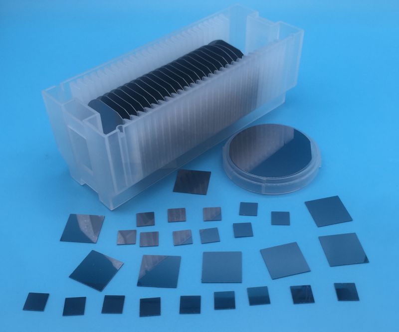
Dimension
Dia50.8x0.5mm,10×10×0.5mm、10×5×0.5mm
According to customer needs, substrates with special orientation and size can be customized.
Surface Roughness
Surface roughness(Ra):<=5 Å
Atomic Particle Microscopy (AFM) test report can be provided.Polishing
One side or two sides
Package
Class 100 clean bag, Class 1000 super clean room
-
Dimension
∅50.8x0.5mm,10×10×0.5mm、10×5×0.5mm
Orientation and size can be customized.