GaAs
Gallium arsenide (GaAs) is a compound synthesized by two elements of gallium and arsenic. It is an important group IIIA and group VA compound semiconductor material.
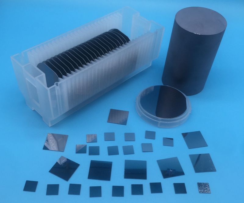
GaAs is a dark gray crystal with metallic shine. It is widely used in infrared optics, optoand microelectronics. Doped crystals of gallium arsenide are used in many applications. The properties of a doped crystal strongly depend on interaction of the doping agent with the intrinsic defects of the crystal. The high silicon doped crystals are used in laser diodes, LEDs, photocathodes and RF generators. GaAs is mostly non-doped in microelectronic applications. GaAs can be grown by Liquid Encapsulated Czochralski (LEC) technology, Float Zone (FZ) method, Vertical Gradient Freeze (VGF) and Horizontal Gradient Freeze (HGF) technology. It is worth noting that only non-doped semi-insulating GaAs is used in optics. In low-power CO2 lasers operating at 9.6-10.6 μm wavelength, gallium arsenide can be an alternative for zinc selenide and can be used for lenses and beam splitters. Due to their nonlinear optic properties, gallium arsenide crystals can be used in therahertz photonics as THz radiation generators.
CasCrysTech (CCT) provides high quality Gallium arsenide (GaAs) crystal which can be customized upon customer's requirements.
Uses/Applications
Gallium arsenide(GaAs) can be used to make microwave integrated circuits, infrared light-emitting diodes, semiconductor lasers and solar cells. GaAs is often used as the base material for the epitaxial growth of III-V semiconductors, including indium gallium arsenide, aluminum gallium arsenide, and so on.
Features/Benefits
▪ Very high electron mobility.
▪ GaAs cells are relatively insensitive to heat compare to silicon cells. Hence it offers high thermal stability.
▪ Lower noise.
▪ Operates over wide temperature range.
▪ High efficiency and resistance to radiation.
-
Single Crystal
Doping
Conductivity Type
Carrier Concentration (cm-3)
Dislocation Density (cm-2)
Growth Method
Standard Substrate
GaAs
None
Si
/
<5×10⁵
LEC
HB
Dia3″
Dia3″×0.5
Dia2″×0.5
Si
N
>5×10¹⁷
Cr
Si
/
Fe
N
~2×10¹⁸
Zn
P
>5×10¹⁷
Dimension
25×25×0.5mm、10×10×0.5mm、10×5×0.5mm、5×5×0.5mm
According to customer needs, substrates with special orientation and size can be customized.
Surface Roughness
Surface roughness(Ra):<=5Å
Atomic Particle Microscopy (AFM) test report can be provided.Polishing
One side or two sides
Package
Class 100 clean bag, Class 1000 super clean room
-
25×25×0.5mm、10×10×0.5mm、10×5×0.5mm、5×5×0.5mm
According to customer needs, substrates with special orientation and size can be customized.