Si
Crystalline silicon material is the most important photovoltaic material, and its properties are gray black with metallic luster, high melting point (1410 ℃), high hardness, brittleness and inactive chemical properties at room temperature. Its market share is more than 90%, and it will still be the mainstream material of solar cells for a long time in the future.
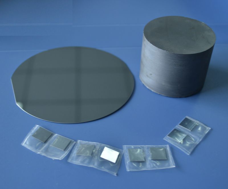
CasCrysTech (CCT) provides high quality silicon wafers which can be customized upon customer's requirements.
Uses/Applications
Crystalline silicon material is the most important photovoltaic material, and it will still be the mainstream material of solar cells for a long time in the future.
Features/Benefits
High hardness, brittleness and inactive chemical properties at room temperature.
-
Crystal Structure
Cubic
Melting Point
1420℃
Density
2.4(g/cm3)
Dopant
Undoped
Boron
Phosphorus
Conduction Type
I
P
N
Resistivity
1000Ωcm
10-3~1000Ωcm
10-3~1000Ωcm
EPD
≤100∕cm2
≤100∕cm2
≤100∕cm2
Oxygen Content(∕cm3)
≤1~1.8×10¹⁸
≤1~1.8×10¹⁸
≤1~1.8×10¹⁸
Carbon Content(∕cm3)
≤5×10¹⁶
≤5×10¹⁶
≤5×10¹⁶
Dimension
5x5mm ,10×10mm, 20×20mm
Ø50.8mm, Ø76.2mm, Ø100mm
According to customer needs, substrates with special orientation and size can be customized.
Thickness
0.5mm、1.0mm
Dimension Tolerance
<±0.1mm
Thickness Tolerance
<±0.025mm
Polishing
One side or two sides
Orientation Tolerance
±0.5°
Edge Orientation Accuracy
2° (Special requirements can reach within 1°)
Orientation
<100>、<110>、<111>
Package
Class 100 clean bag, Class 1000 super clean room
-
Dimension
5x5mm ,10×10mm, 20×20mm; Ø50.8mm, Ø76.2mm, Ø100mm
According to customer needs, substrates with special orientation and size can be customized.
Thickness
0.5mm、1.0mm
Dimension Tolerance
<±0.1mm
Thickness Tolerance
<±0.025mm