LaAlO3
Lanthanum aluminate (LaAlO3) single crystal is currently the most important single crystal material for large-scale high-temperature superconducting thin film substrates. Generally grown by Czochralski method, single crystals and substrates with diameter of 2 inches or more can be obtained. It is well matched with YBaCuO and other high-temperature superconducting materials and lattices, with low dielectric constant, low microwave loss and good thermal stability. Lanthanum aluminate has broad application prospects in the fields of electronics, optics and energy.
For example, in the field of electronics, lanthanum aluminate can be used as a thin film dielectric layer to manufacture ceramic microwave dielectric devices with high dielectric constant; In the field of optics, lanthanum aluminate can be used as a highly transparent ultraviolet light barrier film, which is widely used in optoelectronic devices such as lasers and photoluminescent devices; In the field of energy, lanthanum aluminate can be used as the cathode material of fuel cells to improve the electromotive force efficiency of fuel cells.
Therefore, lanthanum aluminate has broad application prospects and will be widely used in the future.
CasCrysTech (CCT) provides high quality lanthanum aluminate (LaAlO3) crystal which can be customized upon customer's requirements.
Uses/Applications
Making high-temperature superconducting microwave electronic devices (such as high-temperature superconducting microwave filters in telecommunication).
Features/Benefits
Matches well with high-temperature superconducting materials and lattices such as YBaCuO;
Has low dielectric constant and low microwave loss.
-
Crystal Structure
M6(normal temperature)
M3(>435℃)
Lattice Constant
M6 a=5.357A c=13.22 A
M3 a=3.821 A
Melting Point
2080℃
Density
6.52(g/cm3)
Mohs Hardness
6-6.5(mohs)
Thermal Expansion
9.4x10⁻⁶/K
Dielectric Constants
ε=21
Secant Loss(10GHz)
~3×10⁻⁴@300k,~0.6×10⁻⁴@77k
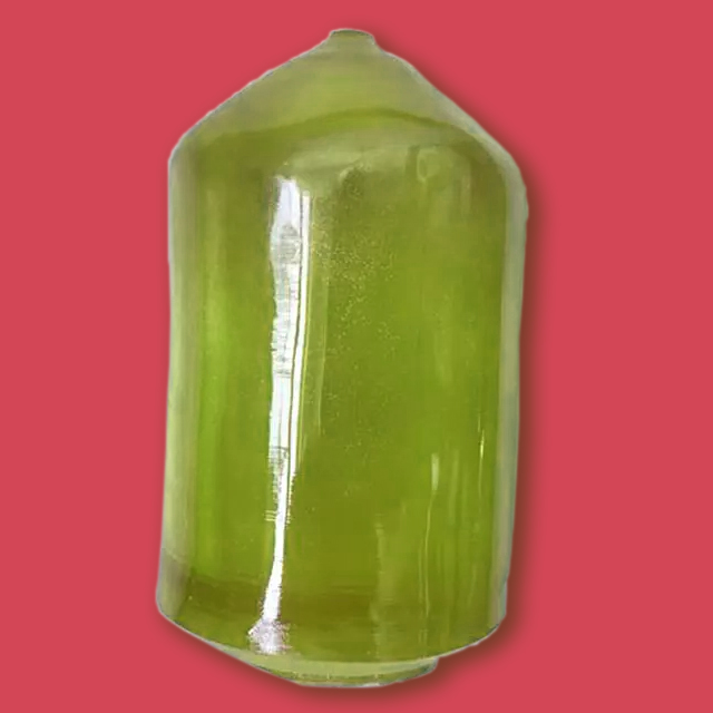
Color and Appearance
To anneal and conditions differ from brown to brownish
The polished substrate has natural twin domains.Chemical Stability
Room temperature is not dissoluble in minerals, the temperature is greater than 150 ℃ in soluble h3po4
Characteristics
For microwave electron device
Growth Method
Czochralski
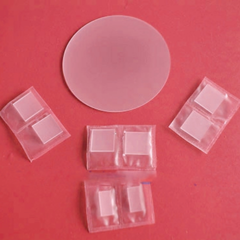
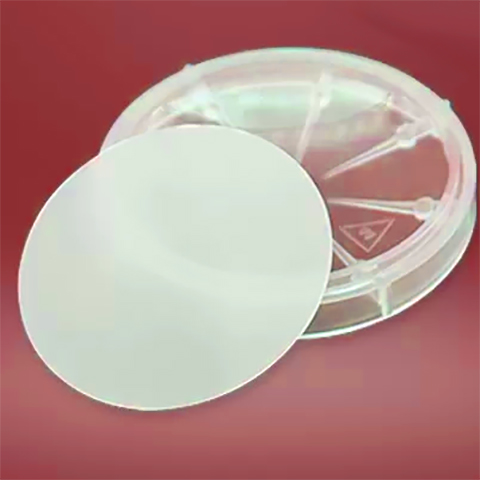
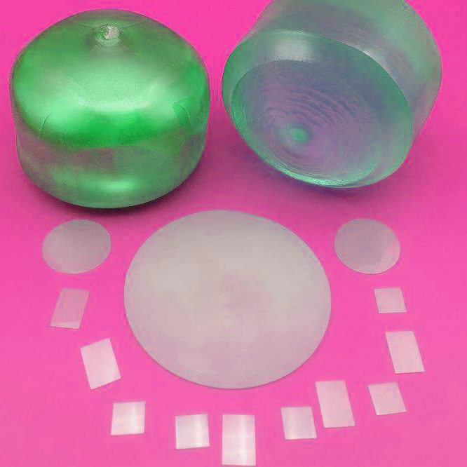
Dimension
10x3mm,10x5mm,10x10mm,15x15mm,20x15mm,20x20mm
Ф15,Ф20,Ф1″,Ф2″,Ф2.6″
Thickness
0.5mm,1.0mm
Polishing
One side or two sides
Orientation
<100> <110> <111>
Crystal Plane Orientation Accuracy
±0.5°
Edge Orientation Accuracy
2°(Special requirements can reach within 1°)
Bevel Wafer
According to specific requirements, wafers with edge-oriented crystal planes inclined at a specific angle (inclination angle 1°-45°) can be processed.
Surface Roughness
Ra≤5Å(5×5µm)
Package
Class 100 clean bag, Class 1000 super clean room
-
Dimension
10x3mm,10x5mm,10x10mm,15x15mm,20x15mm,20x20mm; Ф15,Ф20,Ф1″,Ф2″,Ф2.6″.Thickness
0.5mm,1.0mm