InP
As one of the most important compound semiconductor materials, Indium phosphide (InP) single crystal materials are key materials for the production of InP-based laser diodes (LD), light-emitting diodes (LEDs) and photodetectors in optical communications. These devices realize the emission of information in optical fiber communications, Dissemination, amplification, acceptance and other functions. InP is also very suitable for high-frequency devices, such as high electron mobility transistors (HEMT) and heterojunction bipolar transistors (HBT). Due to its superior characteristics, it is used in optical fiber communication, microwave, millimeter wave, Many high-tech fields such as radiant solar cells and heterojunction transistors. The main growth methods of InP single crystal materials include traditional liquid-sealed Czochralski technology (LEC), improved LEC technology, and gas pressure controlled Czochralski technology (VCZ). /PC-LEC)/Vertical Gradient Solidification Technology (VGF)/Vertical Bridgman Technology (VB), etc.
CasCrysTech (CCT) provides high quality Indium phosphide (InP) crystal which can be customized upon customer's requirements.
Uses/Applications
Key materials for the production of InP-based laser diodes (LD), light-emitting diodes (LEDs) and photodetectors in optical communications.
Suitable for high-frequency devices, such as high electron mobility transistors (HEMT) and heterojunction bipolar transistors (HBT).
Features/Benefits
Indium phosphide (InP) includes phosphorus and indium and is a binary semiconductor. It has a zincblende crystal structure similar to GaAs and almost all the III-V semiconductors.
-
Crystal
Structure
Crystal Orientation
Melting Point oC
Density g/cm3
Forbidden Band Width
InP
Cubic,
a=5.869 Å
<100>
1600
4.79
1.344
Parameters
Single Crystal
Dopant
Conduction Type
Carrier Concentration
cm-3
Mobility (cm2/V.s)
Dislocation density (cm-2)
Standard Substrate
InP
Undoped
N
(0.4-2)´1016
(3.5-4)´103
£5´104
Φ2″×0.35mm
Φ3″×0.35mm
InP
S
N
(0.8-3)´1018
(4-6)´1018
(2.0-2.4)´103
(1.3-1.6)´103
£ 3´104
£2´103
Φ2″×0.35mm
Φ3″×0.35mm
InP
Zn
P
(0.6-2) ´1018
70-90
£ 2´104
Φ2″×0.35mm
Φ3″×0.35mm
InP
Te
N
107-108
³2000
£3´104
Φ2″×0.35mm
Φ3″×0.35mm
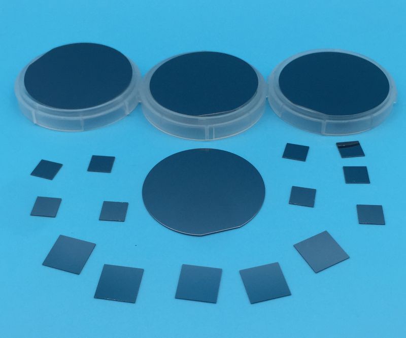
Dimension
Dia50.8x0.35mm,10×10×0.35mm、10×5×0.35mm
Orientation and size can be customized.
Surface Roughness
Surface roughness(Ra):<=5 Å
Atomic particle microscope ( AFM ) test report can be providedPolishing
One side or two sides
Package
Class 100 clean bag, Class 1000 super clean room
-
Dimension
Φ 50.8x0.35mm,10×10×0.35mm、10×5×0.35mm
Customized upon request.